 |
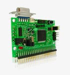
Adapt9S12C is a next-generation version of the immensely popular Adapt11 product originally introduced by Technological Arts in 1994. The flexible design, wide range of connector options, and breadboard pluggability address all facets of training, evaluation, development, prototyping-- and even volume production.
If you are migrating from the 68HC11, you'll appreciate the backward-compatibility. At the same time, you'll love the powerful HCS12 instruction superset, with its advanced DSP-like instructions, 16-bit arithmetic, memory-to-memory moves, and many powerful addressing modes.
Adapt9S12C Highlights:
- based on the Freescale 9S12C MCU (80-pin QFP version)
- includes 8 Mhz crystal
- up to 24 MHz bus speed (via PLL)
- low-dropout 1.5 Amp regulator, selectable for 3.3V or 5V operation (NOTE: when operated at 3.3V, the on-board CAN transceiver is not functional)
- includes RS232 transceiver circuit (9-pin D-sub connector)
- includes CAN transceiver circuit (not functional when board is operated at 3.3V)
- has small footprint (2K) on-chip Serial Monitor for easy code-loading and simple debug capability
- supports standalone operation
- 32K or 128K Bytes Flash
- 2K or 4K Bytes Ram
- standard 50-pin Adapt11 form-factor board (1.7" x 2.8")
- plug it into a solderless breadboard (choose "SB" connector option)
- compatible with Adapt11 backplanes and prototyping cards
- an extra eight I/O pins accessible via auxilliary 10-pin connector
![]()
9S12Cxx Family MCU Features:
Product Details
Ease-of-Use Features:
- supports programming in C, BASIC, Forth, assembler, etc.
- no special Flash programming voltage or switch required
- fast in-circuit programming
- small footprint on-chip bootloader/monitor and free uBug12 GUI for quick loading/debugging of user programs on a WIndows platform
- Run/Load switch for choice of Standalone or Monitor operation
- compatible with virtually all 9S12 development tools on the market
Flash-based code development using on-chip debug/monitor
Flash-based code development using a Background Debug Mode (BDM) pod
-
More Features:
- standard 6-pin BDM connector for full debugging capabilities (when used with an optional BDM pod)
- up to 44 digital I/O lines on primary I/O connector
- eight can be used as 10-bit analog inputs (Port AD)
- auxilliary I/O connector brings out 8 more I/O pins (Port P)
- up to six PWM channels (Port P)
- up to eight Input Capture/Output Compare pins (Port T)
- serial peripheral interface (SPI)
- serial communications interface (SCI)
- controller area network (CAN 2.0) with on-board transceiver circuit
- up to ten key wake-up interrupt pins
- internal programmable pullup and pulldown resistors on most pins
- user access to MCU reset signal
Resources
Module Documentation:
- Adapt9S12C Feature and Pinout Sheet
- Adapt9S12C Manual
- Adapt9S12C Mechanical Drawing
- Adapt9S12C Modular Configuration Examples
- Adapt Family Application Card Pinout Table
Device Documentation:
- MC9S12C Fact Sheet
- MC9S12C Family Product Brief
- MC9S12C Family Data Sheet
- MC9S12CWebpage
- CAN Transceiver Data Sheet
- RS232 Transceiver Data Sheet
- LM1086CT-ADJ Voltage Regulator Data Sheet
Tools and Examples
- uBug12 GUI for working with the on-chip Serial Monitor under Windows and .NET framework (if you need it)
- Linux command line tool hc12mem for working with the Serial Monitor
- SynCode: Free Integrated Editor and GNU C Compiler package for Windows
- Special Edition of CodeWarrior C compiler from Freescale. It has a 32K C code limit, and unlimited assembler!
- 45-day Demo C compiler (ICC V7 for CPU12) from ImageCraft
- Pluto Visual Debugger
- Windows IDE for GNU C
- Using the GNU Development Tools for 68HC11 and 68HC12
- 68HC11/HCS12 Application Notes for ICC and GNU C Compilers
- FreeRTOS for 9S12C
- Karl Lunt's binload utility
- University of Texas Course Notes & Examples